The Best AI Accelerators in 2026: An Expert Comparison of Nvidia, AMD, and Google
Nvidia AI chip dominance faces new pressure in 2026. Compare H100, Blackwell B200, AMD MI300X, and Google TPU on real inference economics. Find out who wins.
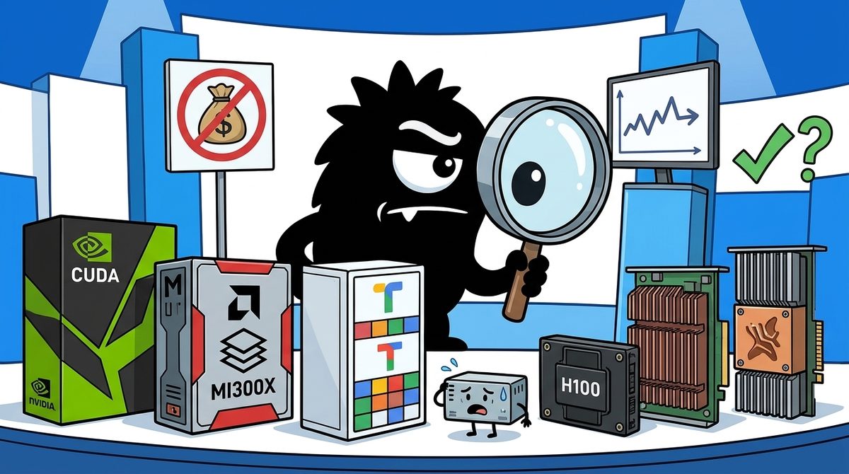
Should you default to Nvidia Blackwell in 2026, or do AMD and Google accelerators now make sense? As of mid-2026, Blackwell (B200, B300, and the rack-scale GB200/GB300 NVL72) is the right default for most production inference. That is especially true if you serve open-weight models that ship in FP4 or run high-concurrency workloads. AMD's MI300X, MI325X, and MI355X are good choices for memory-bound, low-concurrency inference and for cost-sensitive capacity. Google's TPUs make sense mainly if you're already committed to GCP. Secondhand H100s are still useful for budget training.
The more important lesson is about method. The spec sheets you've been comparing are probably measuring the wrong thing.
Bottom line (2026):
- Peak FLOP badly understates Blackwell's inference lead. Modelled serving benchmarks show roughly 10x more advantage than FLOP figures suggest.
- Native FP4 open-weight models favor Blackwell's hardware FP4 support and are speeding up a refresh away from H100.
- AMD wins on memory per dollar and single-user latency. That advantage fades past about eight concurrent users.
- Judge accelerators on tokens per dollar at your real concurrency, not on peak specs.
Nvidia's Dominance Isn't a Rumor — It's a Market Structure
Nvidia's lead is the backdrop to every hardware debate on X right now. Industry estimates put Nvidia at roughly 80% of AI accelerators heading into 2026[3]. CNBC reported in 2024 that the company held the overwhelming majority of the AI chip market even as competitors lined up[1]. The revenue concentration follows from that share. TrendForce found Nvidia commanded about half of the revenue among the top 10 IC design houses in 2024[4]. TechInsights' 2024 ranking put it at the top of the global semiconductor league[5]. Epoch AI's chip market-share tracking by designer shows the same concentration in installed compute[6].
What has changed in 2026 is how fast buyers move between Nvidia generations. In the past, the shift from one default GPU to the next took a year or more. Now it is happening in weeks:
For years, every GPU request I got was for H100s by default. Since last week, every single message has been asking for B200s and B300s.
Kimi K3 and GLM-5.2 ship native FP4 weights. Blackwell runs them in hardware while Hopper has to dequantize on the fly. Roughly 3x better perf per dollar on B200 for the same model.
Open weight models are quietly accelerating Nvidia's next hardware cycle. Nobody buys new H100s anymore; that market is almost entirely secondhand.
Ivan Burazin's point that "nobody buys new H100s anymore" matters more than it first appears. When the market for a flagship part becomes almost entirely secondhand within roughly two years of launch, you're seeing a structural refresh cycle. That cycle is driven by changes in numerical formats and by rack-scale economics. Hype alone doesn't explain it. The rest of this article covers both drivers, because they decide whether a competitor can actually break in.
Why Raw FLOP Numbers Lie About Blackwell
This is the most useful evaluation lesson in the current conversation. FLOP per second (floating-point operations per second) measures peak arithmetic throughput. It doesn't measure how many tokens you can serve. Inference, particularly agentic workloads with long contexts, is limited by memory bandwidth, KV-cache handling (the stored attention state for prior tokens), interconnect, and numerical format. FLOP captures none of those.
Epoch AI made this concrete with an inference index published in late 2025:
Epoch AI published an inference index on November 9 that scores accelerators on modelled agentic serving instead of raw FLOP per second.
The reason for building it is in one line. Epoch estimates the Nvidia GB300 gives about 25 times the H100's inference capacity per chip on the workloads it models. The same part has only 2.5 times the 8-bit FLOP per second. So reading the FLOP figure alone understates the gap by a factor of ten. The modelled job is a long cached context of 262,144 tokens with 1,024 new tokens per prefill. That runs at roughly 1.51 input tokens per output token, across four model architectures.
The scores are normalised so GB300 NVL72 is 1. H200 HGX gets 0.12 and B300 HGX gets 0.54. AMD's MI355X gets about 0.55, which lands it level with the eight-GPU Blackwell Ultra box. Vera Rubin gets 2.18. Epoch puts GB300's 1.9 times lead over B300 HGX down to scale-up domain, since it links 72 GPUs where B300 HGX links 8.
The key figure is that GB300 delivers about 25x H100's modelled inference capacity per chip with only 2.5x the 8-bit FLOP, so FLOP understates the gap by 10x. The workload explains why. A 262,144-token cached context with only 1,024 new tokens per prefill spends most of its time moving cached state, and very little doing fresh math. Larger memory, faster interconnect, and lower precision pay off disproportionately under those conditions. Epoch attributes GB300 NVL72's 1.9x lead over the 8-GPU B300 HGX entirely to scale-up domain: 72 GPUs linked versus 8.
Independent benchmarking of full production inference stacks points the same way:
HOLY CRAP
"Nvidia’s GB300 NVL72 doesn’t disappoint. It achieves up to 100x on FP8 vs FP4 compared to even a strong H100 disagg+wideEP+MTP baseline and 65x on FP8 vs FP8."
"At GTC 2024, Jensen claimed that Blackwell will deliver up to 30x perf on inference compared to H100, Jensen under promised & overdelivered on Blackwell inference performance."
"While performance is competitive on AMD when enabling just a subset of the SOTA inference optimizations, enabling all three major optimizations that labs use, AMD’s performance is currently not competitive with Nvidia’s."
"When it comes to the latest inference techniques that are used by the most prominent frontier large-scale inference services (such as disagg prefill+wideEP+FP4), Nvidia absolutely frame mogs with the B200, B300 and ASU frat leader, rack scale GB200/GB300 NVL72 across both SGLang and TRTLLM. Nvidia GPUs also dominate when it comes to energy efficiency, with much lower all-in provisioned picoJoules of energy per token across all workloads."
The quoted results show up to 100x on FP8-vs-FP4 and 65x on FP8-vs-FP8 over a strong H100 baseline. That baseline already uses disaggregated prefill, wide expert parallelism, and multi-token prediction. Nvidia positioned Blackwell as "born for extreme-scale inference"[10] and claimed up to 30x inference performance at launch[7]. By these measurements, that claim looks conservative.
The caveat matters too. AMD looks competitive when only some state-of-the-art optimizations are enabled. With the full stack that frontier labs use, it does not. Your own results will depend on which of those techniques you actually run.
Native FP4 Weights Are Quietly Rewriting the Hardware Cycle
The hardware story has a software trigger. Blackwell's second-generation Transformer Engine adds native FP4 and FP6 support[8]. Nvidia pitches the DGX B200 around this low-precision inference throughput[9].
Until recently that was a spec-sheet feature with little practical effect. Open-weight models now ship natively in FP4, and that changes the math. Blackwell executes FP4 in hardware. Hopper has to dequantize on the fly, converting the weights back to a higher-precision format before computing. That costs time and erodes the memory savings that justified FP4 in the first place. Burazin's estimate of roughly 3x better perf per dollar on B200 for the same model comes from this gap.
There is also emerging evidence that serious labs run on Blackwell for exactly these workloads:
We (partially) verified these results!
Using NVIDIA B200/H200s, we reproduced the reported patterns for three models.*
We also extended the DeepSeek-V4-Flash test to every weight position across the 42 layers examined and still detected the Blackwell pattern.
See the results here:
https://t.co/TCAfDSGQRx
This is a super clever approach by @willdepue, and matches reporting that top Chinese AI labs are using Blackwells.
* The repo didn’t contain all the inputs needed to test most of the other models
Tim Fist's team partially reproduced a technique that detects a "Blackwell pattern" in model weights. They extended it across all 42 examined layers of DeepSeek-V4-Flash, which is consistent with reporting that top Chinese labs use Blackwell hardware.
This creates a flywheel. When a leading lab chooses a numerical format, it effectively chooses hardware for everyone downstream. Once a popular open-weight model ships in native FP4, every company serving it gains a reason to buy silicon that runs FP4 natively. Nvidia doesn't need to win each procurement fight one at a time. It only needs the formats the ecosystem standardizes on to map well to its tensor cores[12].
For competitors, the question isn't only "is our FP4 fast?" It's "will model producers ship in formats our hardware handles natively?"
AMD MI300X/MI355X: Where It Actually Competes — and Where It Doesn't
AMD gets caricatured on X, either as a "CUDA killer" or as an irrelevance. The benchmark record supports neither view.
The most cited deep dive remains SemiAnalysis's long investigation:
Our 5-month journey conducting independent analysis & benchmarking of AMD MI300X vs Nvidia H100 + H200
Detailed, open source low-level benchmarks
performance vs TCO
Comprehensive public recommendations
It’s not just immature software, they need to change how they do development
Dylan Patel's verdict, "It's not just immature software, they need to change how they do development," is still the sharpest framing. The problem isn't one missing kernel. It's whether optimizations land upstream in the frameworks people use, on the timelines frontier inference demands. The Register's survey of the competitive landscape reached a similar conclusion. AMD's Instinct line is credible hardware competing for a slice of a market where Nvidia's software and systems lead remain the main obstacle[2].
The data does show where AMD competes, and the deciding variable is concurrency, meaning how many requests you batch together:
H100 beats MI355X by 20-30% at batch 1-4. Push to batch 64-128 and that gap shrinks to 5-10%.
At batch 32 on Llama 3.1 70B FP16, estimated numbers from MLPerf data land close: MI355X near 18,000 tokens/s against H100 SXM5 near 19,500. The CUDA advantage is real at low concurrency and mostly disappears once you're running production-size batches.
If your workload runs small batches, the ecosystem gap matters more than the benchmark footnote suggests.
At batch 1–4, H100 leads MI355X by 20–30%. At batch 64–128 the gap narrows to 5–10%. The CUDA advantage is concentrated in low-concurrency serving, where kernel launch overhead and hand-tuned paths dominate. It mostly fades in large batches.
That isn't the whole picture, though, because Blackwell scales differently from Hopper:
Single-user MI355X is the honest headline, but your own load table flips it: B300 hits 1.9x H200 at 16 users and 2.2x at 32, against 1.4x and 1.7x for MI355X. Past eight users the AMD win is gone.
View on XAgainst B300, the curve reverses. MI355X can win the single-user headline, but at 16 and 32 concurrent users B300 pulls ahead: 1.9x and 2.2x over H200, compared with 1.4x and 1.7x for MI355X. Past about eight users, AMD's advantage disappears.
At rack scale on mixture-of-experts (MoE) reasoning models, the gap widens further:
NVIDIA Blackwell vs others.
quite an exhaustive report by Signal65.
"On a per-GPU basis, the MI355X is roughly half the price of the GB200 NVL72 configuration, but since GB200 NVL72 provides a per-GPU performance advantage ranging from nearly 6x at the low end, to as high as 28x at a higher interactivity rate, the NVIDIA platform still offers up to 15x the performance per dollar compared to AMD’s current offering. "
- MoE reasoning makes networking the limiter for inference cost, and claims the rack-scale GB200 NVL72 can hit about 1/15 cost per token on DeepSeek-R1.
Signal65's analysis finds MI355X costs roughly half as much per GPU as GB200 NVL72. GB200 NVL72 delivers 6x to 28x the per-GPU performance depending on interactivity, which works out to up to 15x performance per dollar for Nvidia. The more important point concerns networking. MoE models route tokens across many experts spread over many GPUs, so the scale-up interconnect becomes the bottleneck for inference cost. A 72-GPU NVLink domain is something an 8-GPU node can't match, whatever chip sits inside it.
AMD's honest position in 2026: it is competitive per chip and attractive at low concurrency or for memory-bound work. It is structurally behind on rack-scale MoE serving.
The Metric That Matters: Tokens Per Dollar, Not Peak Specs
Buyers ultimately pay for tokens, so compare on cost per token at a speed your users will accept. Artificial Analysis built its headline metric this way:
Google TPU v6e vs AMD MI300X vs NVIDIA H100/B200: Artificial Analysis’ Hardware Benchmarking shows NVIDIA achieving a ~5x tokens-per-dollar advantage over TPU v6e (Trillium), and a ~2x advantage over MI300X, in our key inference cost metric
In our metric for inference cost called Cost Per Million Input and Output Tokens at Reference Speed, we see NVIDIA H100 and B200 systems achieving lower overall cost than TPU v6e and MI300X. For Llama 3.3 70B running with vLLM at a Per-Query Reference Speed of 30 output tokens/s, NVIDIA H100 achieves a Cost Per Million Input and Output Tokens of $1.06, compared to MI300X at $2.24 and TPU v6e at $5.13.
For Llama 3.3 70B on vLLM at 30 output tokens/s per query, H100 comes in at $1.06 per million input and output tokens. MI300X costs $2.24 and TPU v6e costs $5.13. That is roughly a 2x Nvidia advantage over AMD and 5x over Trillium. Google is pushing more specialized TPU variants to close the gap[13], and TPUs differ architecturally from GPUs in ways that favor tightly integrated, committed workloads[15]. On this off-the-shelf vLLM benchmark, though, Nvidia wins clearly.
A different ranking produces a different winner:
I ranked 8 data centre GPUs for serving inference by what one rental dollar buys in memory and memory bandwidth.
When a model generates tokens, memory decides which models fit on the card and bandwidth sets how fast tokens come out. This leaves out compute and interconnect, which matter more for long prompts and multi-GPU serving.
S
> MI325X: 256 GB at 6 TB/s for $3.10 an hour. The cheapest memory and the cheapest bandwidth of any card here.
> MI300X: 192 GB at 5.3 TB/s for $2.86. Almost the same value, one generation older.
A
> B300: 288 GB, the most memory on a single card. Large MoE models need fewer GPUs per copy.
> H200: 141 GB at 4.8 TB/s for $5.00. The same bandwidth per dollar as the B200 at about 60% of its hourly price.
> B200: 7.7 TB/s for $8.01, the second-fastest memory on the list.
B
> RTX PRO 6000: 96 GB for $2.38. Cheap capacity, but at 1.6 TB/s it's slow on large models.
> H100: $3.94 an hour for 80 GB. The most expensive memory per GB on the list.
C
> L40S: 48 GB at 0.86 TB/s. The lowest hourly price and the highest cost per unit of bandwidth.
The two best-value cards are listed by 3 to 5 providers each. The H100 is listed by 45. Teams whose serving stack runs on AMD are paying the least per gigabyte today.
Ranked by memory and bandwidth per rental dollar, AMD leads. The MI325X offers 256 GB at 6 TB/s for $3.10/hour, and the MI300X 192 GB at 5.3 TB/s for $2.86. The H100 has the most expensive memory per GB on the list. Ilman Shazhaev also notes that the best-value cards are listed by only 3–5 providers each, while the H100 is listed by 45. Availability is part of your total cost of ownership.
How to reconcile the two rankings: memory per dollar tells you which models fit and the ceiling on decode speed. Tokens per dollar at a reference speed tells you what you actually pay once software maturity, batching, and kernels are included. The gap between those two numbers is roughly the cost of the ecosystem. If your team can close that gap through engineering, AMD's raw value becomes real savings.
Training economics are different again:
b200 vs h100 in mlperf training, 64 gpus each: the b200 finished 2.04x and 2.08x faster
on our pricing page a b200 hour is 2.115x an h100 hour. so per finished run it's basically a tie
where the b200 actually wins: a job that needs 2 h100 nodes but fits on 1 b200 node (180gb per gpu). otherwise it's paying ~2% more to finish in half the time
B200 finished MLPerf training runs about 2.04–2.08x faster but rents at about 2.115x the H100 hourly price, so per completed run it's roughly a tie. The clear win is node consolidation. A job that needs two H100 nodes can fit on one B200 node at 180 GB per GPU, which removes inter-node communication entirely. Side-by-side generation comparisons show the same pattern: the Hopper-to-Blackwell advantage is largest where memory capacity and low precision matter[11].
The Engineering Catch: Blackwell Brought NUMA Back Inside the GPU
This is where reading spec sheets and running production diverge. B200 is two reticle-limited dies, built as large as a lithography reticle allows, with 208 billion transistors in total. A 10 TB/s chip-to-chip link called NV-HBI joins them so the package behaves as one GPU[7][8]. Nvidia presents it as unified, and to CUDA it is. Physically, it is not:
A fun realization I had recently: with Blackwell (B200 and B300), we are basically back to solving classic NUMA problems inside a single GPU package.
To software, a B200 looks like one big unified GPU. But physically it is two silicon dies connected by NV-HBI. And while that cross-die link is fast, local HBM is still noticeably closer. If you ignore this, memory-heavy workloads like MoE layers spend half their time pulling weights across the link, which burns latency and power for no good reason.
Pay attention to MegaMoE in DeepGEMM. In fact, CUDA doesn’t have an API to tell you which SM sits on which die, so just measure it directly with a few lines of pointer chasing.
1. Slice the weights in half onto physical memory for each die, and run a persistent scheduler where SMs pull from their local die first.
2. Only steal work across dies if there are at least two full waves of tasks left. Why?
Otherwise, paying the transit latency for small leftovers just isn't worth it. Then, 4D TMA descriptor can do coordinate routing so the inner loop stays completely clean.
The payoff is ~100 W of package power saved and 5-10% higher sustained clocks. (Which can be hundreds of thousands of $$ saved in real deployment).
Vincent Zhong's observation describes NUMA (non-uniform memory access), a problem familiar from multi-socket servers, where memory attached to your own socket is faster than memory attached to another. On B200, each die's local HBM is noticeably closer than the other die's. If MoE layers ignore locality, they can spend half their time pulling weights across the link.
His suggested fixes are instructive. Measure SM-to-die mapping with pointer chasing, because CUDA exposes no API for it. Slice weights per die and use a persistent scheduler that prefers local work. Steal work across dies only when at least two full waves remain. He reports about 100 W of package power saved and 5–10% higher sustained clocks, which adds up to substantial money across a large deployment.
AMD faced the same issue earlier. The MI300X is a chiplet design with compute dies on top of I/O dies, and its memory hierarchy rewards locality-aware kernels:
ive been working on a full architectural visualization for the mi300x card.
this covers everything you need to visually understand about the architecture starting from individual lanesthrough chiplets, compute units, wavefronts, matrix instructions, and the memory hierarchy.
you can rotate and explode the model, inspect components, experiment with execution masks, see how matrix elements map to lanes, and calculate LDS usage for different tile sizes.
there’s also an animated trace following a tile through memory to matrix computation, plus comparisons with H100 to connect familiar NVIDIA concepts to AMD’s architecture.
project link in the comments -
Jino Rohit's interactive breakdown of the MI300X's chiplets, wavefronts, and memory hierarchy, including the mapping to familiar H100 concepts, is a good primer on why this matters for both vendors.
The broader lesson: chiplet scaling moves complexity back onto software[12]. Every vendor is now multi-die, so the moat shifts toward whoever's kernel libraries and inference engines handle locality automatically. Today that favors Nvidia's ecosystem, with libraries like DeepGEMM already doing this work. It is also a place where a determined competitor could catch up.
What's Coming Next — and What Could Finally Loosen Nvidia's Grip
Nvidia's next step is Vera Rubin. In Epoch's index it scores 2.18 against GB300 NVL72's baseline of 1, per the AIQuanting summary above. The more telling detail is why GB300 NVL72 beats B300 HGX: the 72-GPU scale-up domain. The moat in 2026 is the rack, not the chip. Rack-scale NVLink, combined with an inference software stack tuned for disaggregation and wide expert parallelism, is the hardest thing for rivals to copy. Packet.ai's 2026 architecture overview also frames Blackwell's value at the system level[12].
Pressure is still building. Epoch's tracking of AI compute share by designer shows hyperscaler custom silicon and AMD gaining ground[6]. Projections in that conversation have Nvidia's share falling toward the low 60s. Google is launching more specialized TPU variants to compete directly[13]. In June 2026, OpenAI unveiled its first custom chip, built with Broadcom[14]. When the largest buyers design their own silicon, they also define the workloads it serves. That shrinks the addressable market where CUDA's flexibility counts most.
Lock-in is uneven. CUDA's advantage is strongest for novel kernels, research iteration, and low-concurrency serving, where hand-tuned paths matter. It is weakest for stable, high-batch production workloads on mature models, where Spheron's data shows the gap shrinking to single digits. AMD and others have long competed for exactly that slice[2]. The next contest will be over networking and scale-up interconnect, because MoE inference cost is set there.
Who Should Use What: A Practical 2026 Buying Guide
Nvidia Blackwell (B200/B300, GB200/GB300 NVL72): the default for most teams.
- You serve open-weight models that ship in native FP4.
- You run high-concurrency production inference (more than about 8 users per replica), especially MoE.
- You can consolidate a multi-node Hopper job onto one Blackwell node[11].
- Pick rack-scale NVL72 if you run large MoE reasoning models at scale. Pick HGX for 8-GPU-scale serving.
AMD MI300X/MI325X/MI355X: for memory-bound, cost-sensitive teams with engineering depth.
- Single-user or low-concurrency inference where large HBM capacity lets big models fit on fewer cards.
- Capacity-heavy deployments where memory per dollar dominates.
- Only if your team can invest in ROCm tuning and accept thinner provider availability.
Google TPU v6e: for committed GCP shops.
- Teams already on Google Cloud running stable workloads that can be adapted to the TPU stack. Off-the-shelf vLLM economics currently trail Nvidia.
Secondhand H100/H200: for budget training and non-FP4 work.
- Fine-tuning and training where per-run cost is roughly equal to B200 anyway.
- Hopper also remains well-proven for serving FP8 and BF16 models[9]. The H200's bandwidth per dollar is competitive.
Decision checklist:
- What's your real concurrency? Below about 8 users, AMD is competitive. Above it, Blackwell pulls away.
- What format do your models ship in? Native FP4 tips the decision strongly toward Blackwell.
- Does the model fit on one node? Consolidation is often where most of the savings come from.
- Are you comparing on tokens per dollar at a target speed, not peak FLOP?
- Can your team close the ecosystem gap? If yes, AMD's raw memory value becomes savings. If no, you'll pay the difference in engineering time.
Sources
[1] CNBC — Nvidia dominates the AI chip market, but there's rising competition
[2] The Register — AMD Instinct, cloudy silicon vie for a slice of Nvidia's pie
[3] Silicon Analysts — NVIDIA AI GPU Market Share 2026: ~80% of AI Accelerators
[4] EMSNow / TrendForce — Global Top 10 IC Design Houses See 49% YoY Growth in 2024, NVIDIA Commands Half the Market
[5] TechInsights — McClean Report March 2025: 2024 Semiconductor Ranking and Q1 Outlook
[6] Epoch AI — AI chip market share by designer
[7] NVIDIA Newsroom — NVIDIA Blackwell Platform Arrives to Power a New Era of Computing
[8] NVIDIA — Blackwell Architecture
[9] NVIDIA — DGX B200: The Foundation for Your AI Factory
[10] NVIDIA Blog — NVIDIA Blackwell: Born for Extreme-Scale AI Inference
[11] Tensorcore — Hopper vs Blackwell: H100, H200, B200 & B300 Compared
[12] Packet.ai — NVIDIA Blackwell Architecture Explained 2026
[13] The Straits Times — Google escalates Nvidia rivalry with new TPUs
[14] TechCrunch — OpenAI unveils its first custom chip, built by Broadcom
[15] Bloomberg — How Do Google's TPU AI Chips Differ From Nvidia GPUs?
References (15 sources)
- Nvidia dominates the AI chip market, but there's rising competition - cnbc.com
- AMD Instinct, cloudy silicon vie for a slice of Nvidia's pie - theregister.com
- NVIDIA AI GPU Market Share 2026: ~80% of AI Accelerators - siliconanalysts.com
- Global Top 10 IC Design Houses See 49% YoY Growth in 2024, NVIDIA Commands Half the Market, Says TrendForce - emsnow.com
- McClean Report March 2025: 2024 Semiconductor Ranking and Q1 Outlook - techinsights.com
- AI chip market share by designer - epoch.ai
- NVIDIA Blackwell Platform Arrives to Power a New Era of Computing - nvidianews.nvidia.com
- Blackwell Architecture - nvidia.com
- DGX B200: The Foundation for Your AI Factory - nvidia.com
- NVIDIA Blackwell: Born for Extreme-Scale AI Inference - blogs.nvidia.com
- Hopper vs Blackwell: H100, H200, B200 & B300 Compared - tensorcore.si
- NVIDIA Blackwell Architecture Explained 2026 - packet.ai
- Google escalates Nvidia rivalry with new TPUs - straitstimes.com
- OpenAI unveils its first custom chip, built by Broadcom - techcrunch.com
- How Do Google’s TPU AI Chips Differ From Nvidia GPUs? - bloomberg.com
Related Guides

The Best AI Model of 2026: What $4.3M in Polymarket Bets Reveals About the AI Race in 2026
19 min read
n8n vs AgentOps vs Zapier AI: Which Is Best for Business Workflow Automation in 2026?
22 min read
The Best AI Model Tools in 2026: What a $4.3M Polymarket Bet Reveals About the Race
21 min read
The Best AI Model Bet: What Polymarket's 72% Google Odds Reveal for Developers in 2026
18 min read